Forbidden gap

Prabhu TL
1 Min Read
Disclosure: This website may contain affiliate links, which means I may earn a commission if you click on the link and make a purchase. I only recommend products or services that I personally use and believe will add value to my readers. Your support is appreciated!


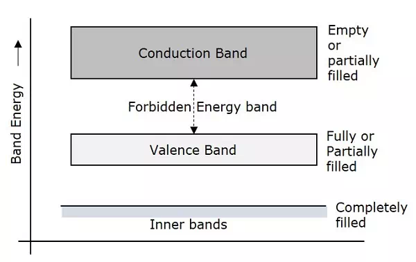
The gap between valence band and conduction band is called as forbidden energy gap. As the name implies, this band is the forbidden one without energy. Hence no electron stays in this band. The valence electrons, while going to the conduction band, pass through this.

The forbidden energy gap if greater, means that the valence band electrons are tightly bound to the nucleus. Now, in order to push the electrons out of the valence band, some external energy is required, which would be equal to the forbidden energy gap.

The following figure shows the valance band, conduction band, and the forbidden gap.

Description: Forbidden Gap

Depending upon the size of the forbidden gap, the Insulators, the Semiconductors and the Conductors are formed.

Share This Article
Prabhu TL is a SenseCentral contributor covering digital products, entrepreneurship, and scalable online business systems. He focuses on turning ideas into repeatable processes—validation, positioning, marketing, and execution. His writing is known for simple frameworks, clear checklists, and real-world examples. When he’s not writing, he’s usually building new digital assets and experimenting with growth channels.
Leave a review