After having known about various components, let us focus on another important component in the field of electronics, known as a Diode. A semiconductor diode is a two terminal electronic component with a PN junction. This is also called as a Rectifier.
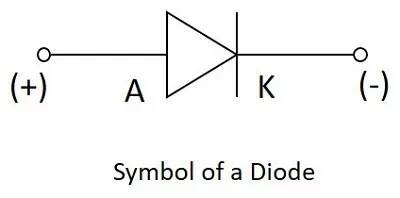
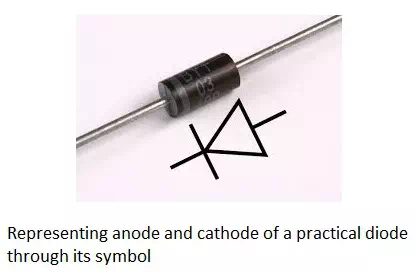
The anode which is the positive terminal of a diode is represented with Aand the cathode, which is the negative terminal is represented with K. To know the anode and cathode of a practical diode, a fine line is drawn on the diode which means cathode, while the other end represents anode.
As we had already discussed about the P-type and N-type semiconductors, and the behavior of their carriers, let us now try to join these materials together to see what happens.
Formation of a Diode
If a P-type and an N-type material are brought close to each other, both of them join to form a junction, as shown in the figure below.
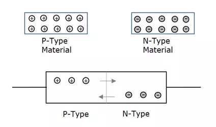
A P-type material has holes as the majority carriers and an N-type material has electrons as the majority carriers. As opposite charges attract, few holes in P-type tend to go to n-side, whereas few electrons in N-type tend to go to P-side.
As both of them travel towards the junction, holes and electrons recombine with each other to neutralize and forms ions. Now, in this junction, there exists a region where the positive and negative ions are formed, called as PN junction or junction barrier as shown in the figure.
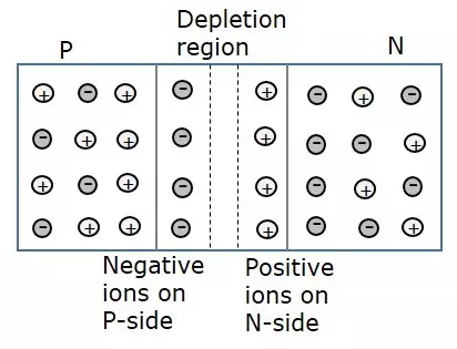
The formation of negative ions on P-side and positive ions on N-side results in the formation of a narrow charged region on either side of the PN junction. This region is now free from movable charge carriers. The ions present here have been stationary and maintain a region of space between them without any charge carriers.
As this region acts as a barrier between P and N type materials, this is also called as Barrier junction. This has another name called as Depletion region meaning it depletes both the regions. There occurs a potential difference VD due to the formation of ions, across the junction called as Potential Barrier as it prevents further movement of holes and electrons through the junction.