
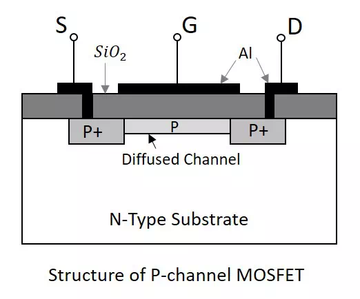
The construction and working of a PMOS is same as NMOS. A lightly doped n-substrate is taken into which two heavily doped P+ regions are diffused. These two P+ regions act as source and drain. A thin layer of SiO2is grown over the surface. Holes are cut through this layer to make contacts with P+ regions, as shown in the following figure.
Working of PMOS
When the gate terminal is given a negative potential at VGG than the drain source voltage VDD, then due to the P+ regions present, the hole current is increased through the diffused P channel and the PMOS works in Enhancement Mode.
When the gate terminal is given a positive potential at VGG than the drain source voltage VDD, then due to the repulsion, the depletion occurs due to which the flow of current reduces. Thus PMOS works in Depletion Mode. Though the construction differs, the working is similar in both the type of MOSFETs. Hence with the change in voltage polarity both of the types can be used in both the modes.
This can be better understood by having an idea on the drain characteristics curve.