

The reason for the controller function is to manage the NAND components and create a standard interface which interfaces well to host systems. There are many popular interfaces today such as Serial ATA (SATA), SD, MMC, USB, PCIe as well as Parallel ATA (PATA, aka IDE).
All of these SSD interfaces have a common controller architecture design in which a controller resides between the NAND memory and the host system. In future articles we will look at the tasks a controller handles, but here we focus on the basic architecture of a generic Solid State Drive (SSD).
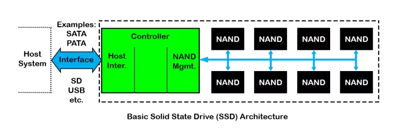
As shown above, the basic SSD consists of a controller chip which manages one or more NAND components, each of which could be comprised of multiple NAND die. The diagram is generic in the sense that it doesn’t matter what final host interface is used.
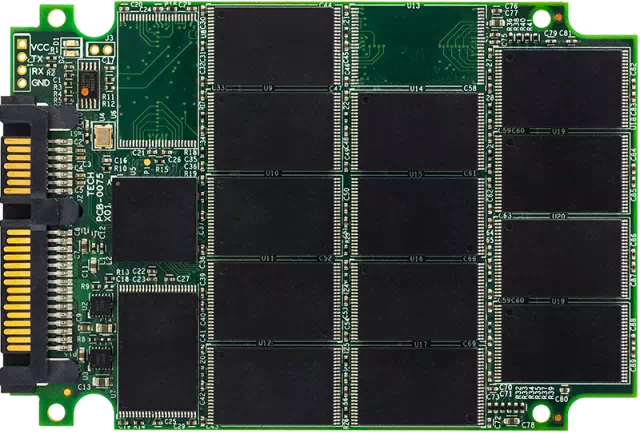
As a real life example, see the image of a SATA SSD’s internal circuit board above. All the rectangular components are NAND chips with the square component as the single controller for this SSD. The controller does not necessarily need to be in a square package, it just happens to be in this case.
Something you’ll notice about this image is how tightly packed the NAND components are to each other. The limitation to an SSD’s storage capacity is how many NAND die can be integrated into the industry standard package along with a controller’s ability to address (read/write) each die.
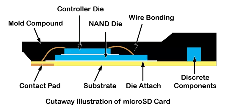
For very small packaged SSD such as microSD cards, there is not sufficient physical space for packaged NAND and controller to be used.

In these cases, the controller die and NAND die are stacked on top of each other and connections are made with wire bonding.
The diagram above only shows a single NAND die in the microSD package, but multiple NAND die can be stacked with the controller to make higher density/capacity parts. The size of the die in the cross section is not proportional to the actual size for clarity. With wafer backgrinding techniques as many 16 NAND die have been successfully integrated into a single microSD card.

