

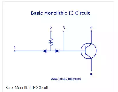
We have already discussed the basics of Integrated Circuits in our previous post. The concepts of a basic monolithic IC will be discussed here. To know the basics a sample circuit must be considered to be converted to its monolithic form. With basic components like resistor, diode, and transistor a basic circuit is first made.
With the basic circuit, the different layers for the monolithic IC are then considered. The basic structure of a monolithic IC will have 4 layers of different materials. The base layer will be a P-type silicon layer and is named as the substrate layer. This layer will have a typical thickness of 200 micrometer. Silicon is the preferred semiconductor for the P-type and N-type layer because of its favourable characteristics for the manufacturing of an IC. The layer above the substrate P-type silicon layer is the N-type layer. All the active and passive components required for the circuit are fabricated onto this layer. This layer has a typical thickness of 25 micrometer. The N-type silicon material is grown as a single crystal extension of the P-layer and the components are required are fabricated using series of P-type and N-type impurity diffusions. The N-type layer becomes the collector for the transistor or an element for a diode or a capacitor.

The layer above N-type is made of silicon dioxide (SiO2) material. Since there is a selective P-type and N-type impurity diffusion going on in the second layer, this layer acts as a barrier in the process. This layer is etched away from the region where diffusion is desired to be permitted with photolithographic process. The rest of the wafer remains protected against diffusion. This layer also protects the silicon layer from contamination. The up-most layer is that made of aluminium. This metallic layer is used to provide interconnections between the different components used in the IC.


