
The Transistor is a three terminal solid state device which is formed by connecting two diodes back to back. Hence it has got two PN junctions. Three terminals are drawn out of the three semiconductor materials present in it. This type of connection offers two types of transistors. They are PNPand NPN which means an N-type material between two Ptypes and the other is a P-type material between two N-types respectively.
The construction of transistors is as shown in the following figure which explains the idea discussed above.
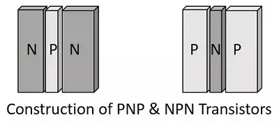
The three terminals drawn from the transistor indicate Emitter, Base and Collector terminals. They have their functionality as discussed below.
Emitter
· The left hand side of the above shown structure can be understood as Emitter.
· This has a moderate size and is heavily doped as its main function is to supply a number of majority carriers, i.e. either electrons or holes.
· As this emits electrons, it is called as an Emitter.
· This is simply indicated with the letter E.
Base
· The middle material in the above figure is the Base.
· This is thin and lightly doped.
· Its main function is to pass the majority carriers from the emitter to the collector.
· This is indicated by the letter B.
Collector
· The right side material in the above figure can be understood as a Collector.
· Its name implies its function of collecting the carriers.
· This is a bit larger in size than emitter and base. It is moderately doped.
· This is indicated by the letter C.
The symbols of PNP and NPN transistors are as shown below.
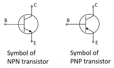
The arrow-head in the above figures indicated the emitter of a transistor. As the collector of a transistor has to dissipate much greater power, it is made large. Due to the specific functions of emitter and collector, they are not interchangeable. Hence the terminals are always to be kept in mind while using a transistor.
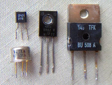
In a Practical transistor, there is a notch present near the emitter lead for identification. The PNP and NPN transistors can be differentiated using a Multimeter. The following figure shows how different practical transistors look like.
We have so far discussed the constructional details of a transistor, but to understand the operation of a transistor, first we need to know about the biasing.